Photonics Systems Group Inaugurates New India Application Center in Pune
New technology hub opens for customer sample testing, live laser depaneling trials, and co-engineering support for India’s electronics manufacturing industry.

Pune, India – 16 July 2026 – Photonics Systems Group has successfully inaugurated its new India Application Center in Pune, marking an important milestone in the company’s expansion in India and its commitment to supporting the country’s rapidly growing electronics and semiconductor manufacturing ecosystem.
The inauguration event, held on 15 July 2026, brought together customers, industry professionals, technology experts, network partners, and representatives from Indian and German institutions. The event featured a live technology showcase of the DP1010 High-Speed Laser Depaneling Machine, demonstrating advanced laser depaneling capabilities for high-precision PCB manufacturing.
The new Pune Application Center is now officially open for customers to bring their own PCB samples, conduct live trials, evaluate process results, and work directly with PSG engineers to develop optimized laser depaneling processes for their specific production requirements.
Speaking at the inauguration, Dr. Marcus Rennekamp, CEO of Photonics Systems Group, emphasized India’s transformation into a leading electronics and semiconductor manufacturing hub.
“India has changed dramatically over the last decade. It has become one of the world’s fastest-growing and leading electronics and semiconductor manufacturing ecosystems. The India of today is a place where innovations are born,” said Dr. Rennekamp.
He further highlighted the increasing need for advanced manufacturing solutions as electronic products become smaller, more complex, more sensitive, and more valuable across industries such as automotive, medical, aerospace, and defense.
“Traditional manufacturing systems often bring stress into delicate products or are not able to meet the requirements for cleanliness and precision. Therefore, the time could not be better for bringing the laser micromachining technology stack to India,” he added.

The DP1010 High-Speed Laser Depaneling Machine showcased during the event reflects PSG’s German engineering expertise and is designed to support stress-free, high-precision PCB separation. Laser depaneling enables non-contact processing, helping manufacturers reduce mechanical stress, improve cutting quality, and process increasingly complex and sensitive electronic assemblies.

A key purpose of the new Application Center is to provide customers with direct access to PSG’s laser micromachining expertise and process development capabilities. Customers can now visit the Pune facility with their own samples, observe the process in detail, try different process setups live, and receive sample results and application reports.
“Seeing is believing. Our Application Center is designed for customers to bring their own PCB samples and co-engineer with PSG’s engineers. Before deciding on a process, customers know exactly what they get,” said Dr. Rennekamp.
Eckhard Schaefer, Vice President Asia of Photonics Systems Group, also addressed the audience and underlined the strategic importance of India for PSG’s regional growth. He emphasized the company’s commitment to providing local expertise, application knowhow, responsive service, and long-term customer support in India and across Asia.
The Pune facility will also support customers who are scaling production over time. PSG’s modular machine portfolio allows manufacturers to start with standalone systems and later upgrade toward automated mass production setups. This approach enables customers to begin with a smart investment and expand as production volumes and requirements grow.

“With PSG, customers can start smart and grow fast,” Dr. Rennekamp noted. “We see ourselves as a long-term engineering and technology partner, not only for a single project.”
With the opening of PSG India, customers in India will benefit from local technical support, spare parts availability, faster service response, application testing, and lifecycle support for laser depaneling equipment.
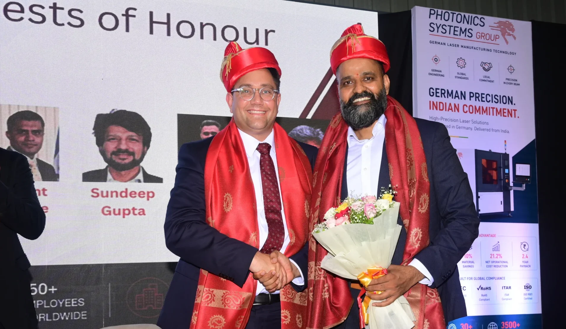
Dr. Rennekamp also thanked Priyant Mane, Managing Director India, and the PSG India team for their dedication in establishing the new center in Pune and transforming the facility into a modern technology and engineering hub.
“Today we inaugurate an Application Center. Tomorrow, we begin solving manufacturing challenges together. We hope this facility becomes a place where ideas are tested, processes are refined, partnerships are built, and innovation moves from concept to production,” he said.
The inauguration was well received by attending customers and industry partners, with strong interest in live machine demonstrations, application discussions, and future sample testing opportunities.
Customers interested in evaluating laser depaneling technology or testing their PCB samples are invited to contact Photonics Systems India to schedule a visit to the Pune Application Center.